
Photo/Yang Qifei (NBD)
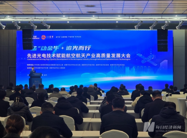
Chengdu introduced specific new measures in early 2026 to deepen the integration between its optoelectronics and aerospace industries, announced at the 'Advanced Optoelectronic Technology Empowering High-Quality Development of Aerospace Industry' conference in its Jinniu District.
The core new measures include establishing a 5 billion yuan parent fund to form a financial empowerment matrix exceeding 20 billion yuanand launching a Semiconductor Packaging & Testing Verification Public Service Platform.
These initiatives aim to provide full-chain capital and technical support, accelerating the application of advanced photonics as the 'core sensing center' for aerospace. Multiple industrial projects were signed, leveraging the district's cluster of over 120 optoelectronic and satellite application enterprisesand a over 40 billion yuan aerospace information industry.
Q:What specific new measures has Chengdu recently taken to promote the integration of optoelectronic technology and aerospace industry?
A: At the 'Advanced Optoelectronic Technology Empowering High-Quality Development of Aerospace Industry' conference held in Chengdu's Jinniu District on January 17, 2026, the city announced several concrete new measures to propel Chengdu optoelectronics aerospace integration. The cornerstone is a financial empowerment strategy centered on a major fund.
Jinniu District officially released a 5 billion yuan mother funddedicated to high-quality industrial development. This fund is designed to amplify into a mother-child fund cluster exceeding 20 billion yuan, creating a full-lifecycle financial support system from seed to merger & acquisition to provide 'relay-style' funding for R&D, pilot testing, and mass production. Another key measure is the launch of a technical support platform.
The district initiated a Semiconductor Packaging & Testing Verification Public Service Platform. This platform, based on domestically developed equipment and expert teams, offers enterprises comprehensive services including chip analysis, failure analysis, and reliability testing, aiming to reduce innovation costs and build a common technical support system.
Furthermore, the integration drive was advanced through project signings. Multiple optoelectronics industrialization projects spanning the upstream, midstream, and downstream of the industry chain were signed during the conference, targeting products, modules, and device packaging to enhance the ecosystem's completeness.
These new measuresare built upon Jinniu District's established industrial foundation, which includes national-level research institutes and growing tech firms in precision optics and infrared detection, and its existing cluster of over 120relevant enterprises.

 川公网安备 51019002001991号